|
Project
Partners
Publications
Legal notice
Private |
|
III-V Lab legal entity
III-V Lab is an industrial Research Laboratory created in 2004 by Alcatel-Lucent and Thales.
Alcatel-Lucent is one of the leaders in communication technologies (mobile, fixed, IP and Optics technologies), applications and services,
while Thales is a major electronic systems company acting in areas such as defence, aerospace, airlines security and safety, information technology, and transportation.
In 2010, III-V Lab was extended with the entrance of the "Laboratoire d'Electronique et de Technologie de l'Information" (LETI) from CEA in the capital, as well as 20 people from the LETI,
opening the way to hybrid III-V on Si integration. CEA is one of the largest public research organisations in France, acting mainly in the fields of low carbon energies, information technologies,
health technologies, large research infrastructures and global security.
Under the guidance of its members, III-V Lab conducts R&D activities in the field of micro/nano-electronics and photonics semiconductor components for different applications
telecoms, space, defence, security, safety, etc.
Lithography facilities | 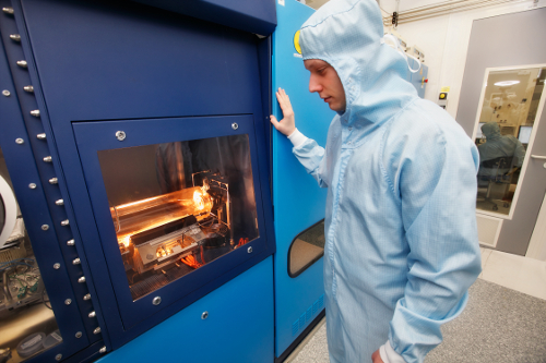
MOVPE G3/2400 Aixtron system |
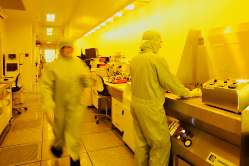
Located on 2 sites near Paris (Marcoussis and Palaiseau), its facilities include 4,000 m2 of clean rooms. Due to the wide range of optoelectronic and electronic devices developed for the needs of its mother companies,
the III-V Lab technology platforms are equipped with a large variety of equipments and the main industrial III-V processing techniques are developed and mastered.
High resolution X-ray diffraction (Panalytical X'Pert) | 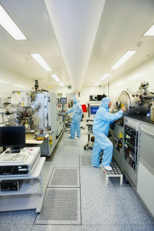
Denton coating facilities for anti-reflection coating on the devices |
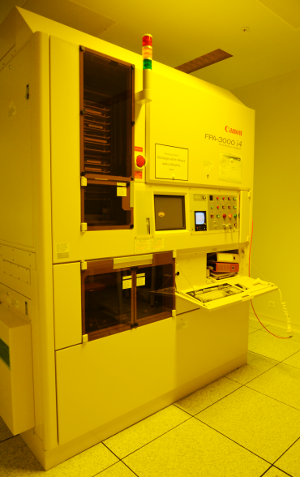
Optical i-Line Canon Stepper FPA 3000 i4 | 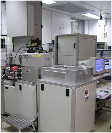
ICP-RIE for the etching of the epilayers for laser fabrication |
III-V Lab staff is composed of around 100 permanent Researchers, plus around 25 PhD students.
III-V Lab master the different steps needed to manufacture III-V components from design to characterisation, including growth and processing.
III-V Lab main tasks in LAMA project
III-V Lab is project coordinator and responsible for Distributed Feedback (DFB) Lasers emitting at 852nm and 894nm delivery to the project partners.
Its technical work is splitted into the following tasks:
- Design of laser structures
- Epitaxy of GaAs based laser heterostructures
- Realisation of the built in Bragg grating for single frequency emission
- Processing, coating and mounting DFB Ridge waveguide lasers emitting at 852nm and 894nm
- Characterisation of DFB lasers
- Ageing study of DFB lasers
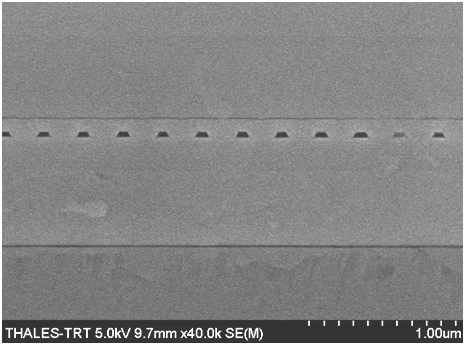
Scanning Electron Microscopy picture of the built in Bragg grating | 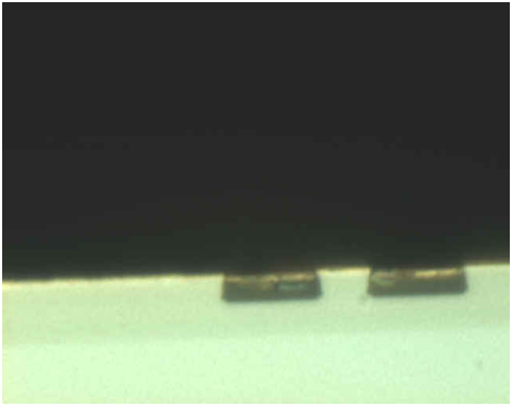
Scanning Electron Microscopy picture of the Ridge waveguide |
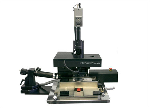
Finetech Fineplacer Lambda equipment for device soldering | 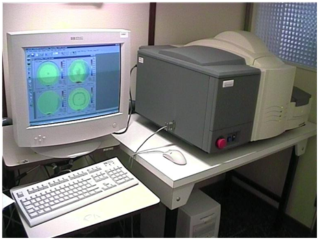
Room temperature PL spectroscopy |
|

